PCB Manufacturing for Beginners: A Step-by-Step Guide

Embarking on the journey of Printed Circuit Board manufacturing may seem like stepping into the realm of intricate electronics wizardry, but fear not, fellow beginners! In this step-by-step guide, we’ll demystify the process, breaking it down into manageable chunks. Whether you’re a budding electronics enthusiast or a curious mind exploring the world of PCBs, let’s dive in!
Understanding the Basics
What is a PCB?
Before we plunge into the manufacturing process, let’s grasp the essence of a PCB. A Printed Circuit Board is the unsung hero of your electronic devices, providing a platform for connecting various components like resistors, capacitors, and integrated circuits. Think of it as the central nervous system of your gadgets, directing the flow of electrical currents.
Types of PCBs
PCBs come in different flavors, each tailored to specific needs:
Single-sided PCBs: Components are mounted on one side of the board.
Double-sided PCBs: Components adorn both sides, connected by through-holes or vias.
Multi-layer PCBs: Sandwiches of copper and insulating layers, ideal for complex circuits.
Now, let’s unravel the manufacturing magic!
Step 1: Designing the PCB
Schematic Design
The journey begins with a schematic—a visual representation of your circuit. Numerous software tools like Eagle, KiCad, or Altium Designer assist in crafting this electronic blueprint. You’ll place components, draw connections, and ensure everything aligns with your circuit’s requirements.
Layout Design
Once your schematic is ready, it’s time for the layout design. This step involves arranging components on the PCB, considering factors like signal integrity, heat dissipation, and overall efficiency. Don’t be afraid to experiment and iterate until you find the perfect arrangement.
Step 2: Generating Gerber Files
What Are Gerber Files?
Gerber files are the universal language of PCB manufacturing. They contain all the information manufacturers need, detailing the layers, traces, pads, and more. Your PCB design software can generate these files, ensuring a smooth transition to the manufacturing phase.
Check, Double-Check, and Triple-Check
Before exporting Gerber files, perform thorough checks. Ensure all components are correctly placed, connections are intact, and there are no floating elements. A meticulous eye here saves headaches later.
Step 3: PCB Prototyping
Why Prototype?
Prototyping is the dress rehearsal before the big show. It allows you to test your design in the real world, uncovering potential issues and refining your circuit.
Printing the Circuit
Manufacturers use various methods like milling or photoengraving to recreate your design on a physical board. The result is a prototype ready for testing.
Assemble and Test
Once your prototype arrives, it’s time to solder components onto the PCB. Embrace your inner scientist, connect the circuits, and power up your creation. This phase is all about spotting issues, tweaking components, and ensuring your circuit dances to your tune.
Step 4: Preparing for Production
Choose Your PCB Manufacturer
With a battle-tested prototype, it’s time to choose a PCB manufacturer. Numerous options cater to different needs and budgets. Popular choices include JLCPCB, PCBWay, and Advanced Circuits. Research, read reviews, and find the best fit for your project.
Review Manufacturer Specifications
Different manufacturers have varying capabilities and requirements. Check their specifications for preferred file formats, layer limitations, and any specific guidelines. This ensures your design aligns seamlessly with their production processes.
Step 5: Submitting Your Design
Prepare Your Files
Go back to those trusty Gerber files. Package them neatly, ensuring you include all necessary layers. Most manufacturers provide detailed instructions on file submission; follow them diligently.
Selecting Options
Manufacturers offer customization options like board thickness, copper weight, and surface finishes. Tailor these to suit your project’s needs. Do you need a gold finish for added durability, or is a standard lead-free HASL (Hot Air Solder Leveling) coating sufficient?
Review and Confirm
Before hitting that submit button, review your order. Confirm your chosen specifications, quantities, and any additional services you might need, such as panelization or electrical testing.
Step 6: Manufacturing
Fabrication Process
Once your design is in the hands of the manufacturer, the fabrication process begins. It involves creating the actual PCB from the materials specified in your design, typically fiberglass and copper.
Layer Alignment and Bonding
In the case of multi-layer PCBs, layers are aligned and bonded together. This ensures seamless connectivity between them.
Copper Etching
Copper layers undergo an etching process, removing excess copper and leaving behind the traces that form your circuit.
Drilling and Plating
Precision is key here. Holes are drilled for components and vias, and plating is applied to create a conductive surface within these holes.
Mask Application and Silkscreen Printing
Solder mask is applied to protect the PCB and define where components will be soldered. Silkscreen printing adds labels and markings to guide assembly.
Quality Checks
Manufacturers conduct rigorous quality checks throughout the process to catch any defects or deviations from your design.
Step 7: Assembly
Gather Your Components
While the manufacturer works on the PCB, it’s time to gather your electronic components. This includes resistors, capacitors, ICs, and anything else specified in your design.
Soldering Time
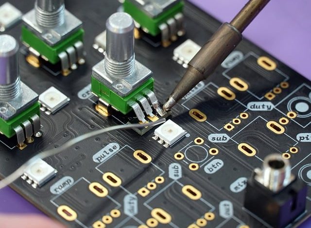
Once your PCBs arrive, the assembly process kicks in. Place components on the board, aligning them with the markings on the silk screen, and solder them in place.
Testing, Testing, 1-2-3
With components securely attached, it’s testing time. Power up your PCB, run functional tests, and ensure everything behaves as expected.
Step 8: Debugging and Iterating
Spotting Issues
Not everything goes perfectly on the first try, and that’s okay. Use your debugging skills to identify and address any issues that arise during testing.
Iterate and Refine
The beauty of PCB design is its iterative nature. Don’t be afraid to go back to the drawing board, make improvements, and order another batch if needed.
Conclusion: Celebrate Your Success
Congratulations, you’ve navigated the intricate landscape of PCB manufacturing! Whether you’re crafting a prototype for personal projects or gearing up for mass production, understanding each step empowers you to bring your electronic dreams to life. Embrace the learning process, celebrate your successes, and keep tinkering. The world of PCBs is yours to explore!


